Here is an introduction of making a GPSDO.
Features
- This GPSDO is fully original and almost totally from scratch design.
- FLL and PLL hybrid control system.
- Display the frequency of estimations.
- Uses some modules that they can buy from the AliExpress stores and these effects of easy construction and good reproducibility to achieve excellent characteristics.
- Displays many diagnosis information on 20×4 lines LCD.
- Uses high precision 32 bits but reasonable price Audio DAC.
- Supports both OCXO and Rubidium Oscillator their support EFC(Electrical Frequency Control).
- Accurate 1.0Hz square pulse output.
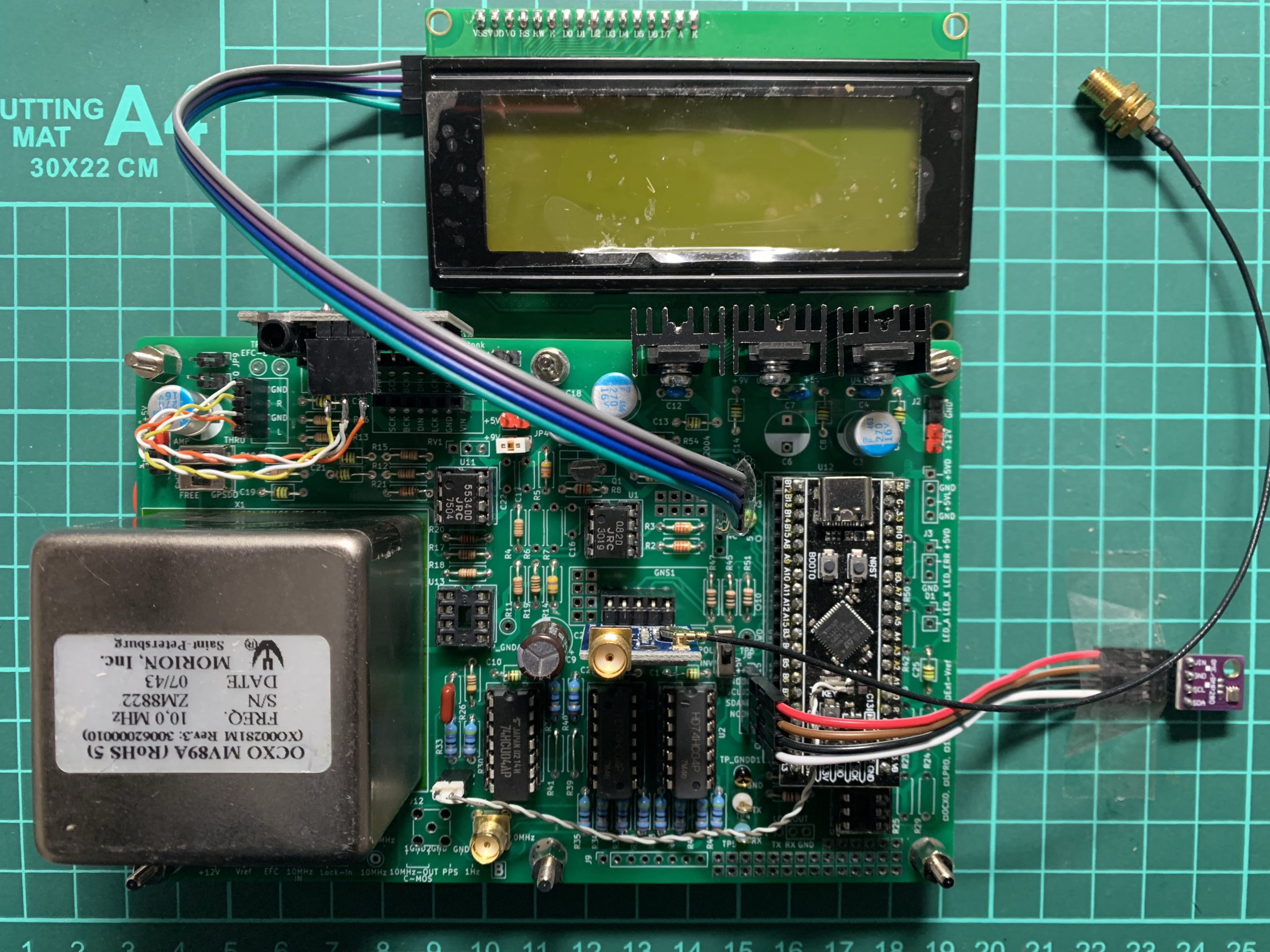
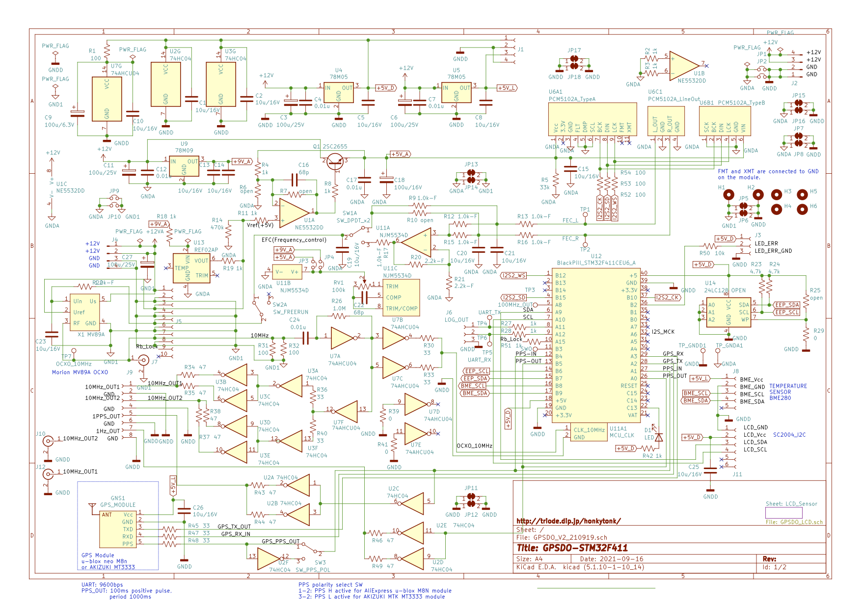
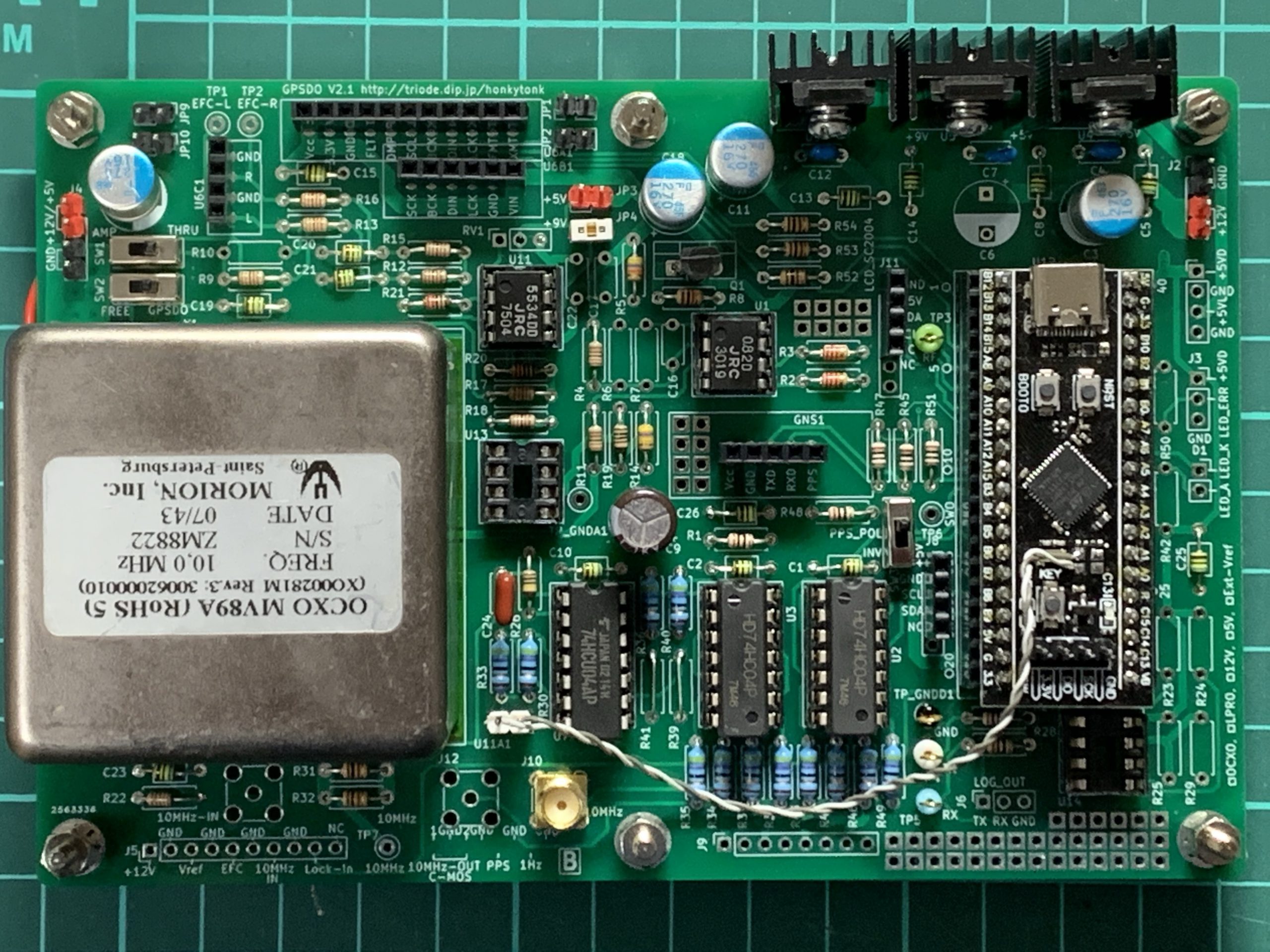
Schematic diagram
- The GPSDO schematic,
 GPSDO_Schematics_V2
 - The GPSDO schematic diagram does not include C-MOS square wave to SIN wave converter/filter, splitter and 50ohm drivers. Supports two channels 10MHz 5V C-MOS level square wave outputs.
Firmware
- I provide 2 firmware releases for UTC and JST time zones.
GPSDO_FW_V103
If you require binary for another time zone, please ask by email at honkytonk.jp[at]gmail.com. - You have to prepare Debug I/F likes ST Microsystems ST-Link V2, ST-Link V3/Set or equivalent.
PCB Gerber data
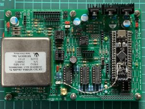
- This GPSDO circuit is simple because of it uses some module boards. So you can easy to make the GPSDO on a 2.5mm pitch universal PCB. I made two GPSDOs by this way.
- I designed the PCB artwork and made trial PCB by ALLPCB.
There are still some mistakes on silk prints, but if you need the Gerber file of the PCB, please ask by email at honkytonk.jp[at]gmail.com.
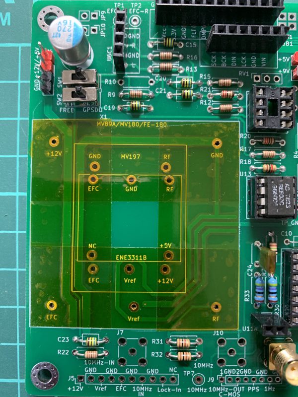
The PCB size is 100mm x 150mm, t = 1.6mm.
Main components
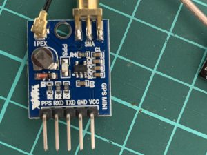
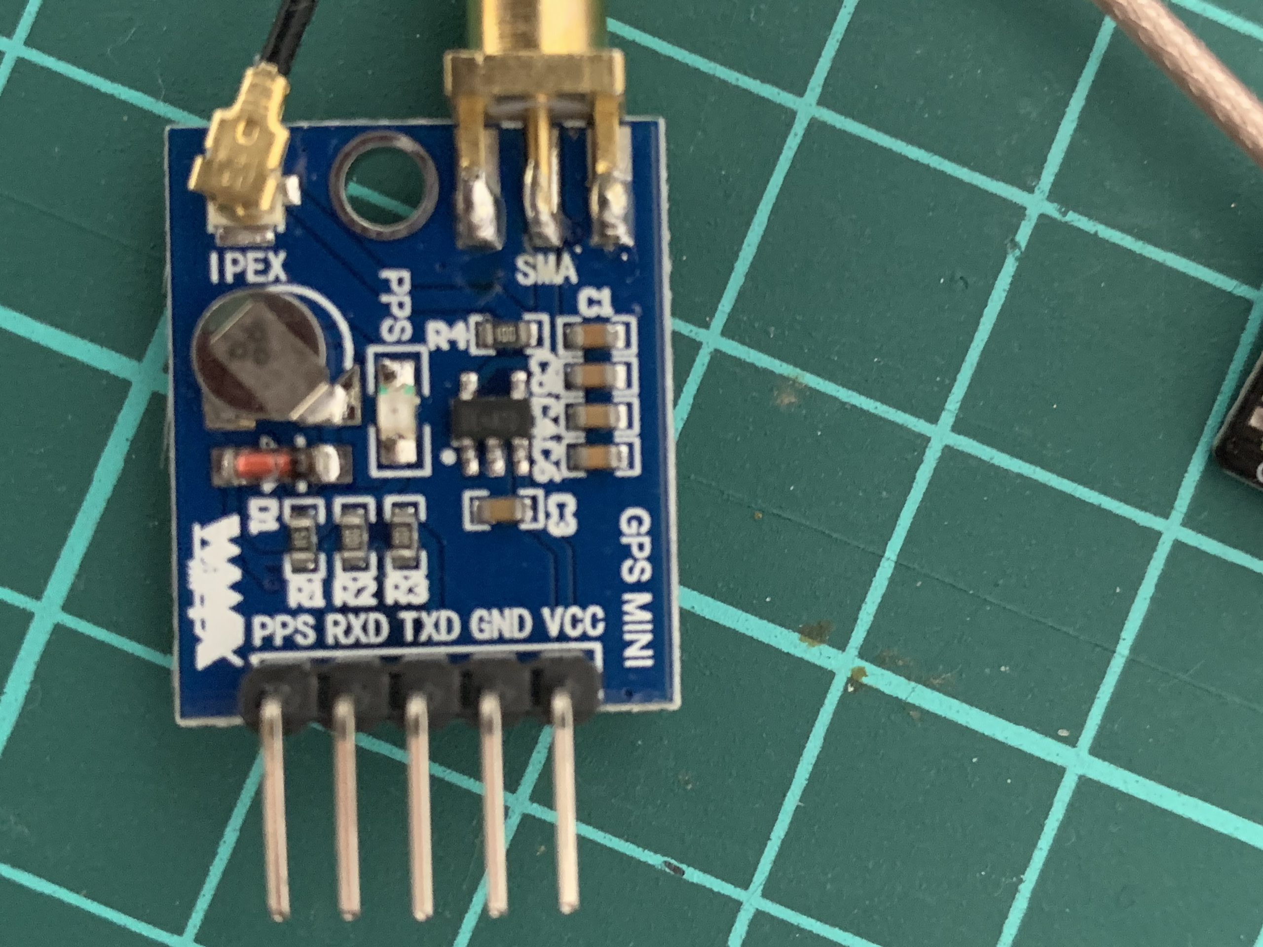
- GPS module:
It is recommended to use the Icofchina ATGM332D or ATGM336 module.
You can use u-blox M8N module and MediaTek MT3333 module.
Please check it supports PPS output. Pin assignments are Vcc, GND, TXD, RXD, PPS.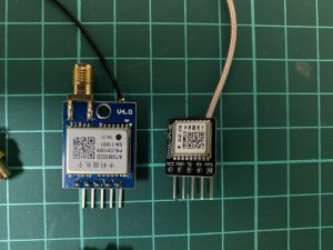
- MCU module:
STM32F411CEU6 Black pill. I recommend to use straight type pin header for SWD I/F.
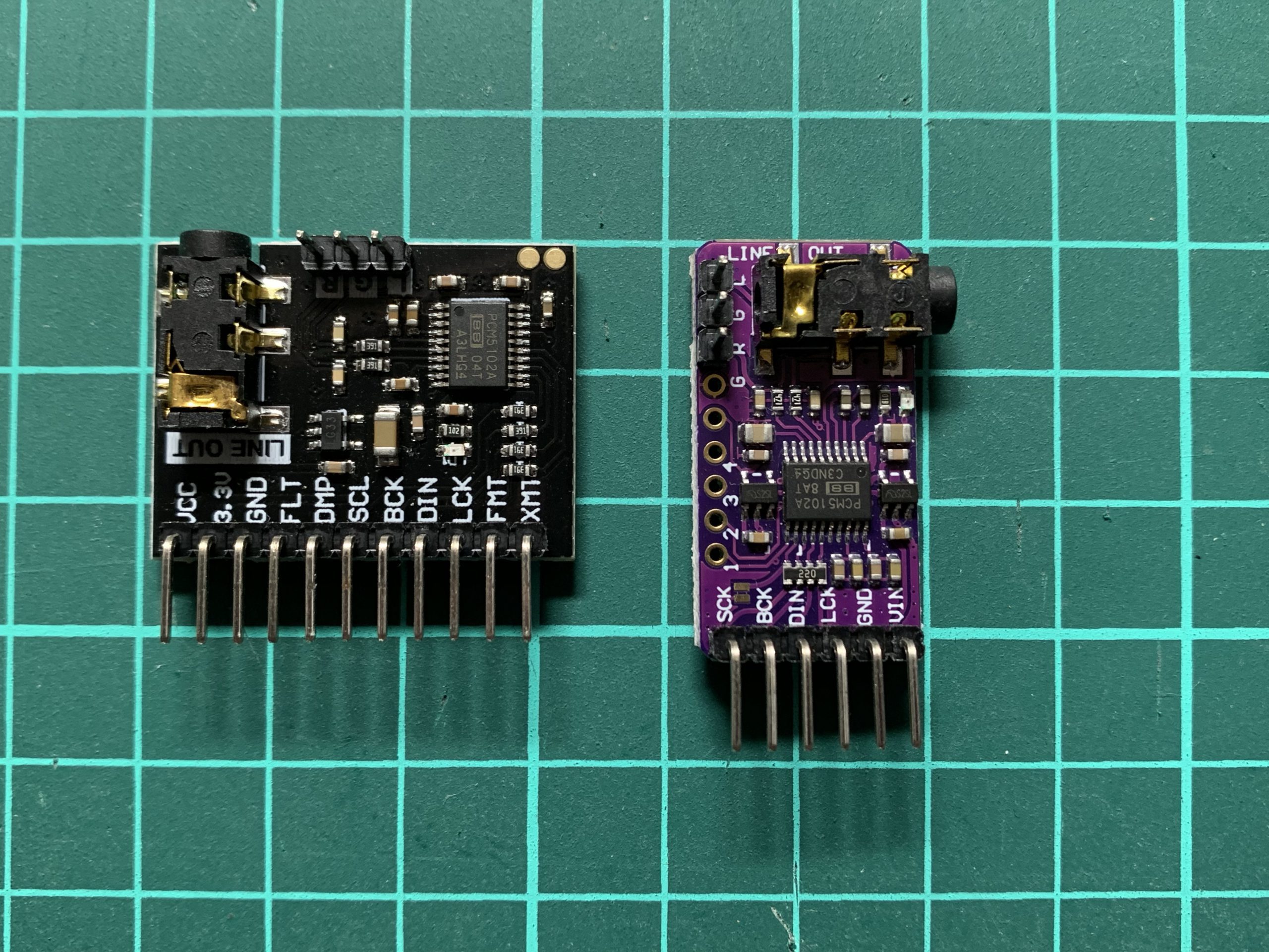
If you use side type one, will be less or tight space to write F/W. - DAC module:
U6A1(or 6B1) PCM5102A Audio DAC module. 2 types module are on the AliExpress store. Both types can be used.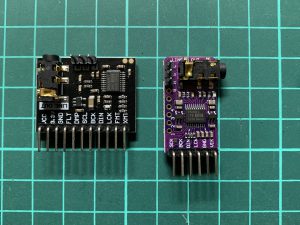 The GPSDO uses the DAC as 19 bits resolution DAC.
 - OCXO:
Highly recommends Morion MV89A, also can use FE-180 or equivalent OCXO. - LCD Display module:
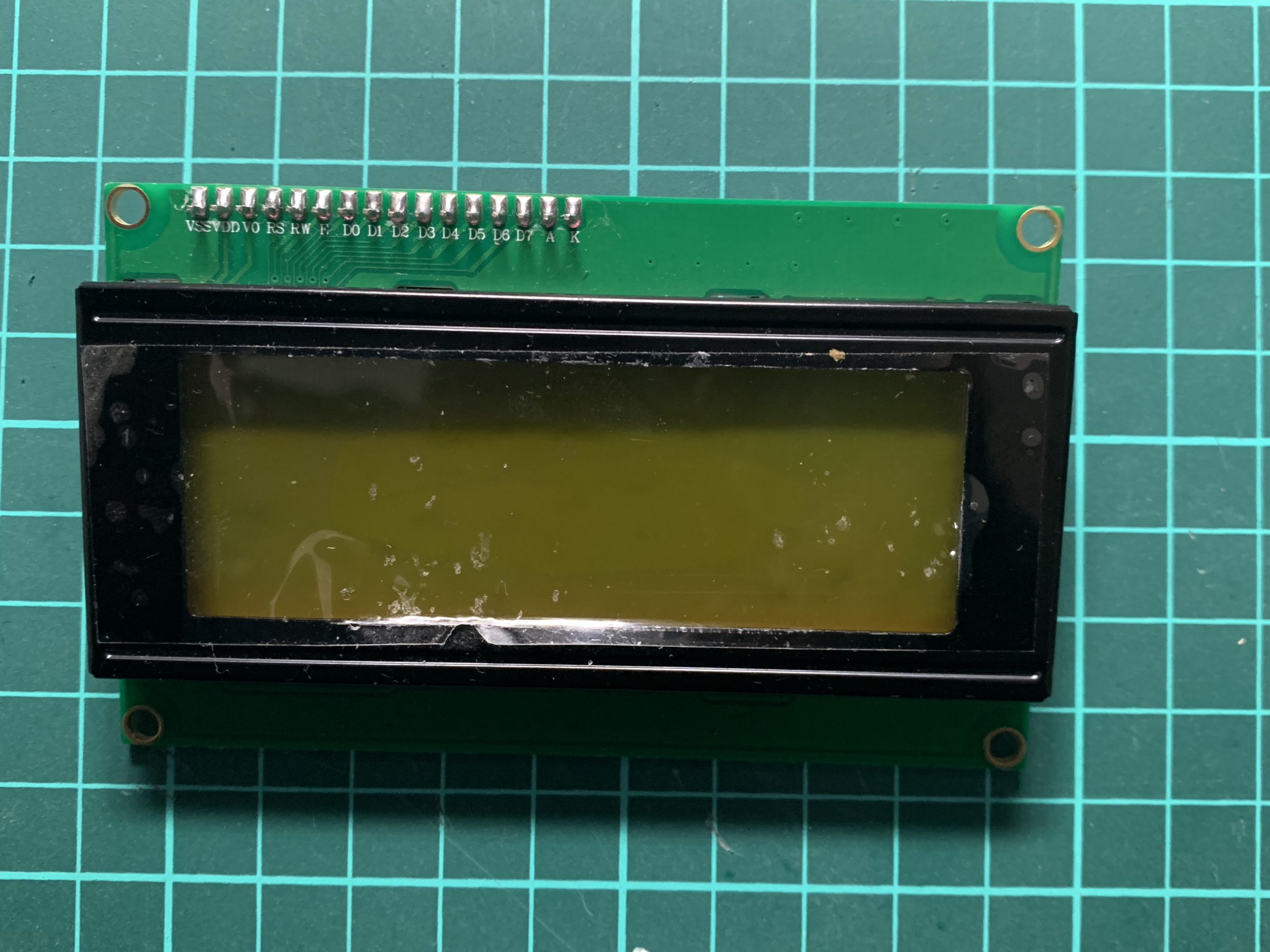
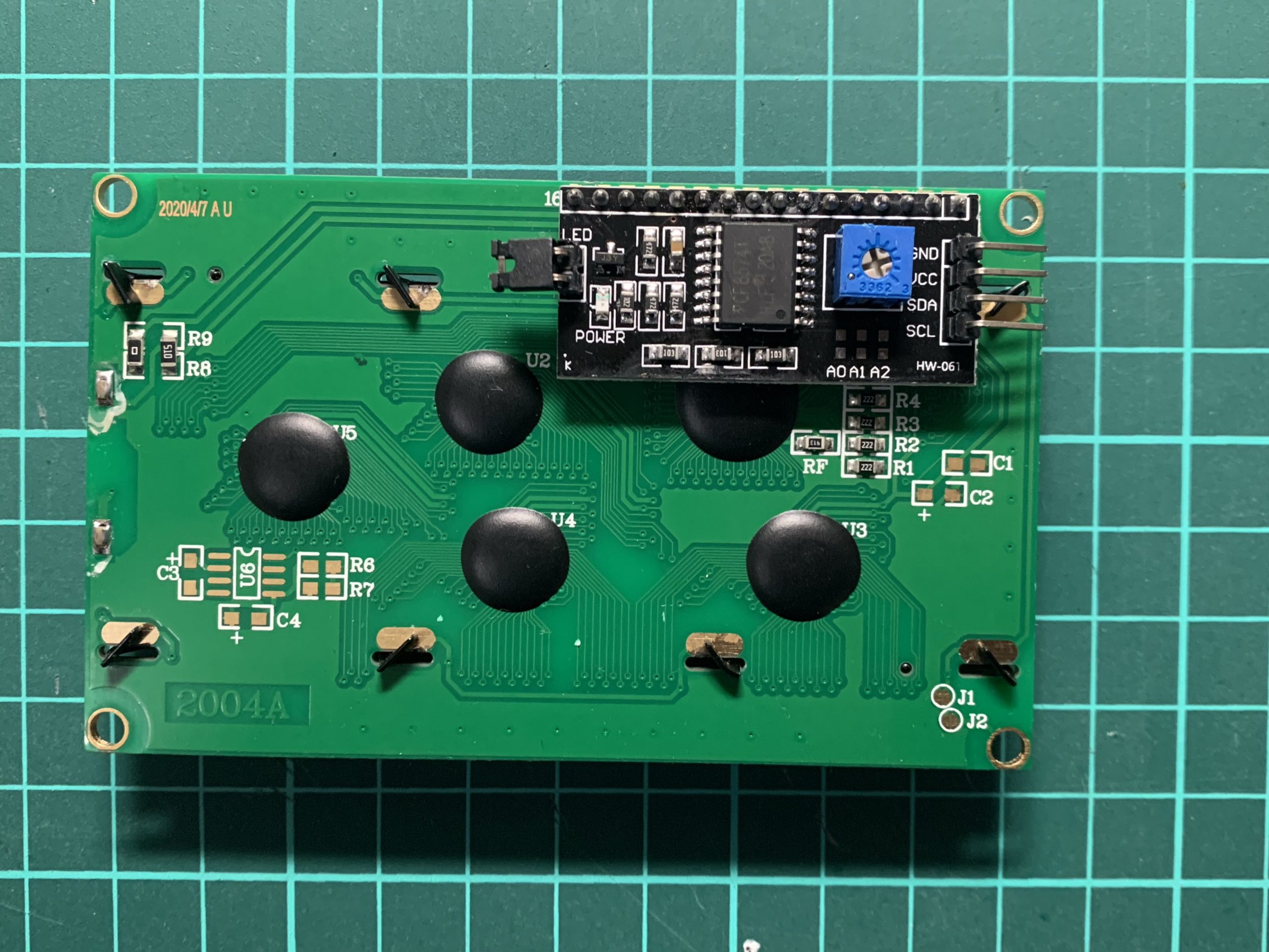
LCD2004 with IIC/I2C I/F board. It can display 20 charactors x 4 lines.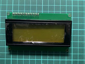
20 x 4 lines LCD Module

I2C I/F on back.
- OP Amp:
U1 : Standard type OP-Amp for analog +5V like NJM5532DD.
U11: Low noise and low drift OP-Amp for EFC buffer like AD4522-1 or NJM5534DD.
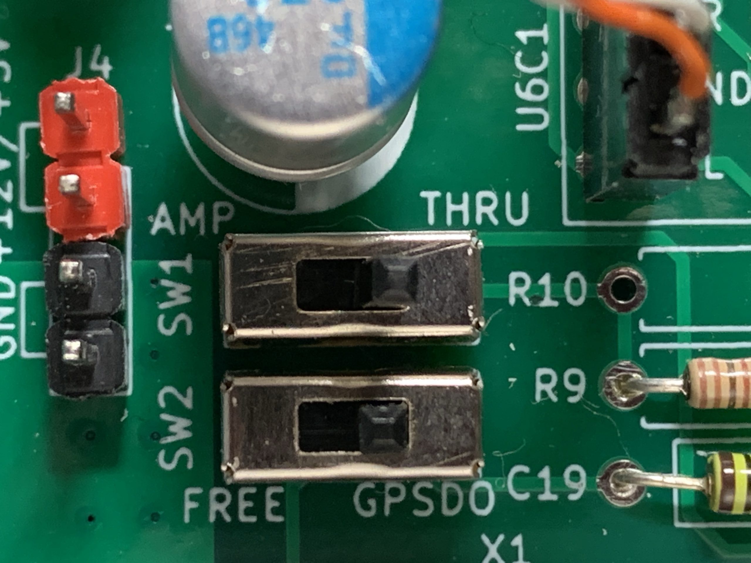
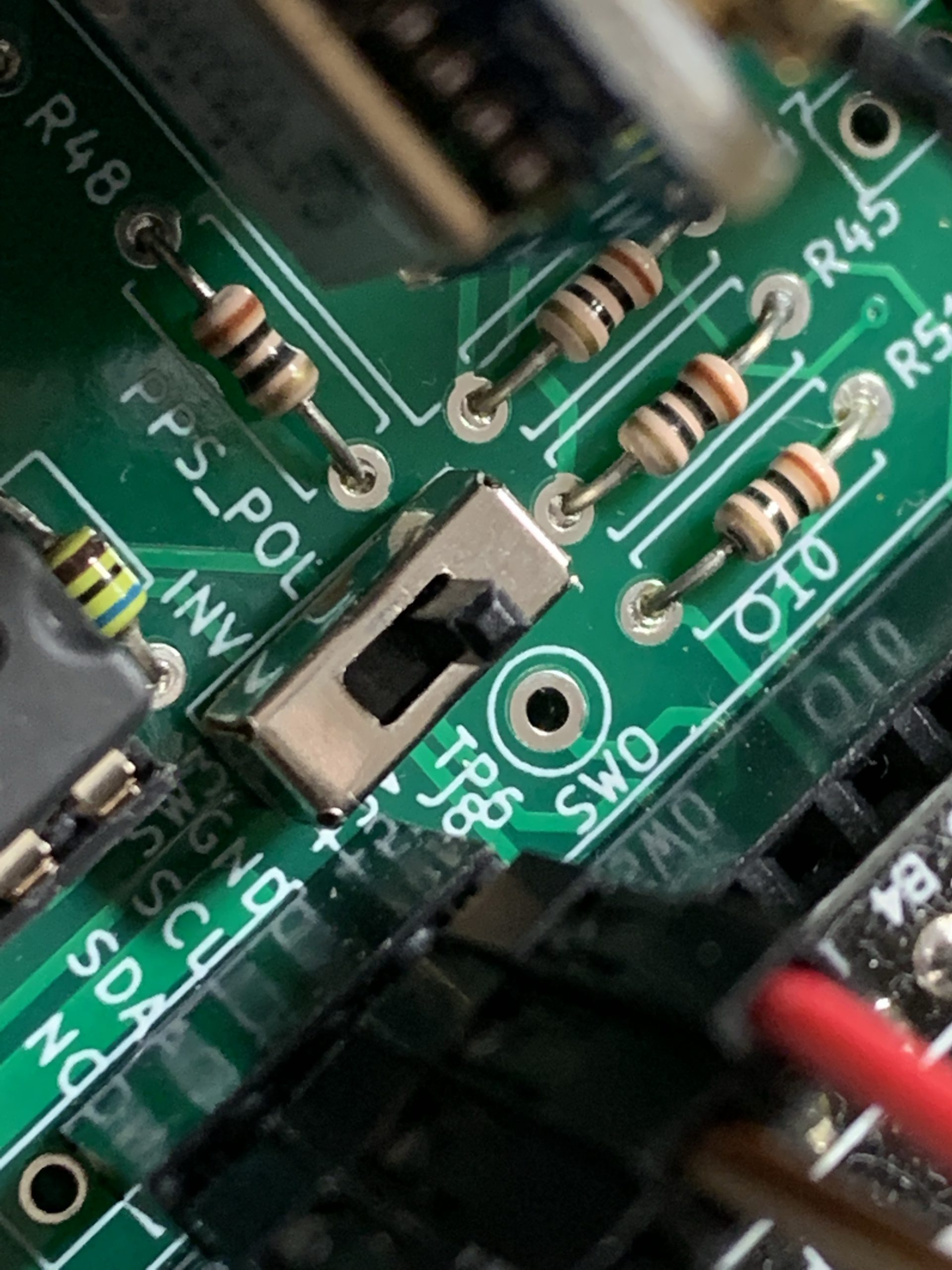
If your OCXO can adjust frequency 10.000000MHz by EFC voltage range from 0 to around 2.7 V, you can reduce the OP-Amp, U11. In this case, pass the buffer circuit by SW1A select 1. - Temperature sensor module: OPTION
Bosh BME280 module to monitor temperature of an enclosure or the OCXO.
This BME280 module is used for displays temperature only, not relates control sequence so far.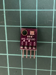
You cannot use BMP280 or others. - Reference voltage IC:
If you use MV89A or equivalent OCXO which supports REF(+5V) output, you don’t need the IC U13, please keep open.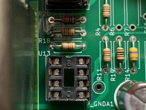
- NVRAM(EEPROM):
Keep open U14. The PCB supports EEPROM circuit but current F/W doesn’t support to store or recall setting parameters from it. - ICs and Transistors:
U7 is 74HCU04, U2 and U3 are 74HC04, Recommend 74HCU04 for U7, not 74HC04.(“U04” means un-buffer type)
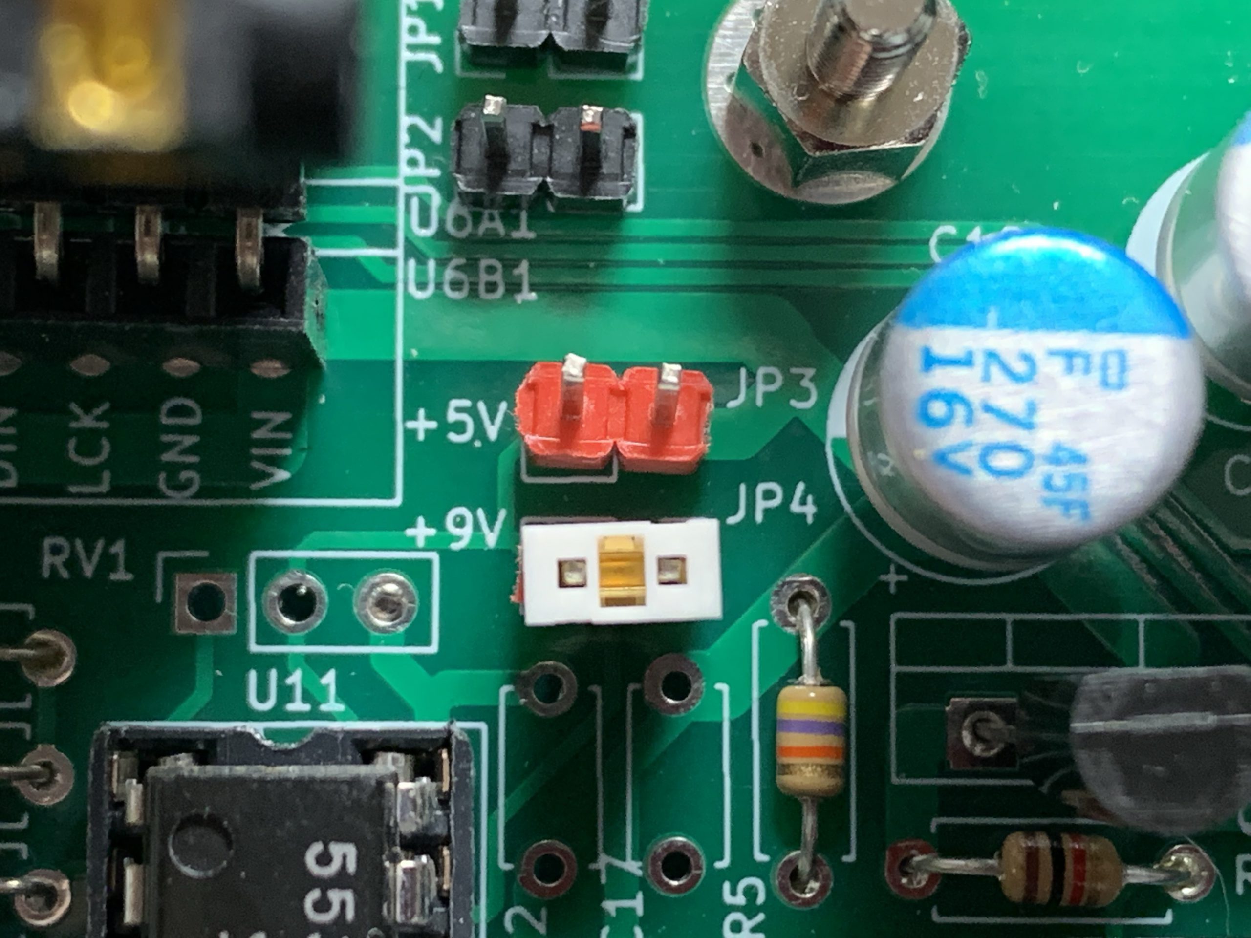
Q1 2SC2655, you can use NPN transistor same rank IC 1A and PC 1000mW instead. Also can use N-ch FET. Please be careful to check the pin assignment. - Regulator ICs:
Silk prints +9 and +5V are mistaken.
Standard linear regulator, U4 and U5 are 7805 and U9 is 7809. You can use 500mW type 78M05 and 78M09 instead. - Enclosure box:
The enclosure is important for ensuring good stability and accuracy for a standard frequency oscillator.
Airflows around the OCXO and electrostatic or electromagnetic interference, etc., cause frequency drift.
The enclosure prevents of them.


Other components
- 1/4 or 1/6W 5% tolerance carbon resistors for non-marked on the schematic.
- 1/4 or 1/6W 1% tolerance metal film resistors for EFC circuit, they are marked “-F” on the schematic.
- Multi layer type ceramic capacitor 10uF/16V. If you can’t purchase this type of capacitors, you can use 0.1uF/50V ceramic capacitor instead. In that case, please add an electric capacitor parallel 100uF/16V to C5 and C8.
- 2.54mm pitch 20pins x 2 line header pin socket for MCU module.
- 2.54mm pitch single line header pin and socket.
My policy is, socket use for outputs and header pin for inputs like power supply.
Recommends to use RED colored header pin for power lines plus +12V. To prevent mis-connection.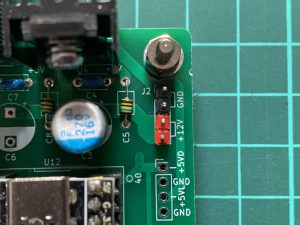
- IC sockets:
To prevent from ESD or other damage. Recommends to use IC sockets, 8 pins for OP-Amps and 14 pins for Logic ICs. Do not set/insert ICs until voltage confirmation completed. - Slide SW:
Small type 2.54mm pitch 1 circuit with 2 selection. - Heat sink:
For 5V and 9V voltage regulator 7805 and 7809.

Preparation before assemble PCB
- Remove a x’tal on the MCU board and small 2 ceramic chip capacitors for the x’tal.
To remove the X’tal, add some solder on it and keep heating by soldering iron then remove it by a tweezer.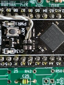
- Add twisted paired wires to the removed pads of the x’tal, these are connected to #2 pin of MCU and GND. Please check which pads are connected where by a tester. In my case, please see a photo below.(the white wire is connected to MCU clock in and the gray one is connected to GND.)
10.0MHz OCXO clock is converted from SIN wave to C-MOS level square wave by IC7 and feeds to MCU via the wires. - Add Kapton (polyimide) tape to avoid short-circuiting by the OCXO body, see photo below,
 The picture is a previous version of the PCB, but almost identical.
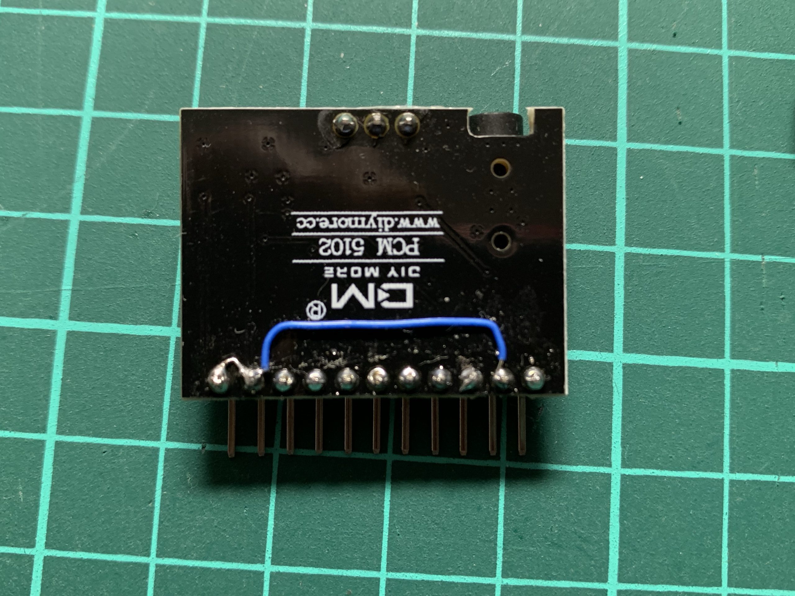
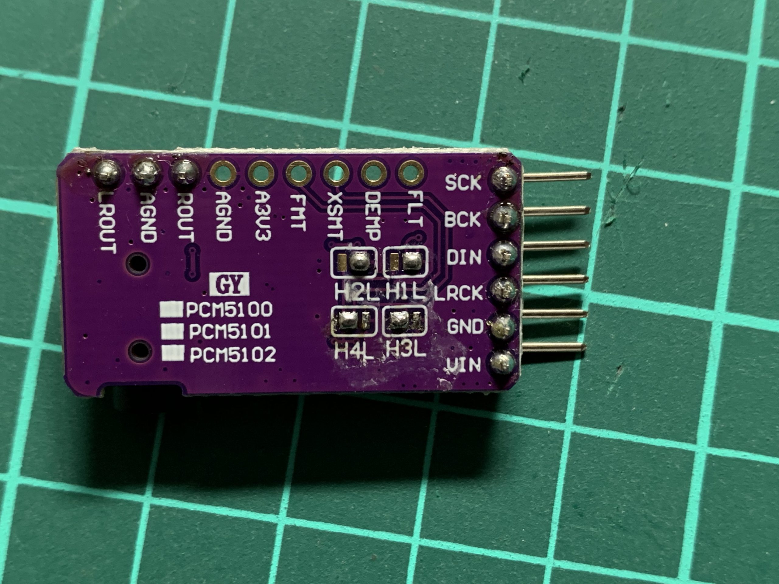
 - Modify the DAC module as below photos.
Connect FMT and XMT pin to Vcc(+3.3V).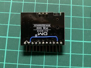
Connect XMT and FMT to 3.3V
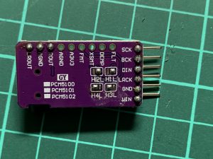
Change solder pads #3 and #4 from L to H.
Prepare to connect from the module L, R outputs to U6C1 by wires.

Start assemble PCB
- Check carefully components polarity, direction and pin assignment of ICs, Transistor and Electrical Capacitor.
- Check carefully soldering not short to neighbor pins.
- Does not solder OCXO at this moment. It solders after voltage check is completed.
- Following components are not used, keep open.
R6, R7, R10, R23, R24, R25, R29, R50
C16, C17, C22,
RV1, U13, U14, - Following resistors are short wire jumpers.
R41, R39 - Following sockets or connectors are option.
J7, J6, J3, J5
In case you require UART logs, please use J6.
Check assembled PCB
After all assembly is completed, let’s start check voltage.
Follow below steps.
- Before turning on power supplies,
Check carefully parts polarity, direction and pin assignment of ICs, Transistor and Electrical Capacitor. - Not insert ICs, except voltage regulator IC 7809 and two 7805s.
- Not insert all modules, MCU, GPS, LCD, DAC and Temperature sensor.
- Not insert OCXO.
- Supply +12V from J2 and J4. It is preferable to reduce the current limit setting of the power supply less than 30mA, if the power supply supports this function.
Then turn on the power supply. If the power supply’s current limiter is working, shut down the power immediately, then check parts mis-direction or soldering etc., - Connect a tester’s Black(-) wire to PCB GND. Check voltage of all logic ICs #14 pin are +5V, voltage of DAC Vcc is +5V, OP Amps voltage 9V or 5V, it depends on JP3, JP4 selection.

Selected 9V
GPS module Vcc is +5V.
- After complete these check. Turn off the power and insert/set all ICs, modules, MCU and OCXO. Please be careful the LCD and the temperature sensor module are used same 4 wire cable but pin assignments are different. If you mis-connected, the modules will be broken.
- Turn off the power to write firmware.
Preparation to write a firmware to MCU.
- Recommends to use ST original debugger I/F ST-Link V2 or ST-Link V3SET. But a cheap Chinese ST-Link adapter which has been sold on AliExpress maybe works, too.
- In case of you use the ST original debugger I/F, first turn off the power then connect debugger cable to SWV connector, next turn on the +12V power then write F/W by STM32CubeProgrammer S/W.
- [IMPORTANT] In case of you use the Chinese cheaper ST-Link. It supplies +3.3V from USB on a PC to SWV connector. Thus turn off the power before connecting the debugger I/F to avoid power line conflicts. It would be more safe to remove MCU board from the PCB…
Start program the firmware.
- Execute STM32CubeProgrammer then push “Open file”, tab file selection dialog will open. Select a binary file then “Open”. Push “Download” button.
- The F/W programming be succeeded, turn off the power and remove SWV cable.
Finally start the GPSDO!
- Connect GPS antenna then place it good sky view location.
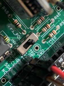
- Set and confirm slide SWs position, SW1: THURU(1), SW2: GPSDO(1), SW3: NORM(1).

- Turn on the power. A start screen is displayed on the LCD and then the MCU LED blinks.
- During the search of GPS satellites, the LED will continue to flash 50% service and its period is 1 sec.
And “Waiting PPS…” message will be displayed on the LCD. - When the GPS Module locks, the LED blink pattern changes to 10% and 90%.
Detail of Display information.
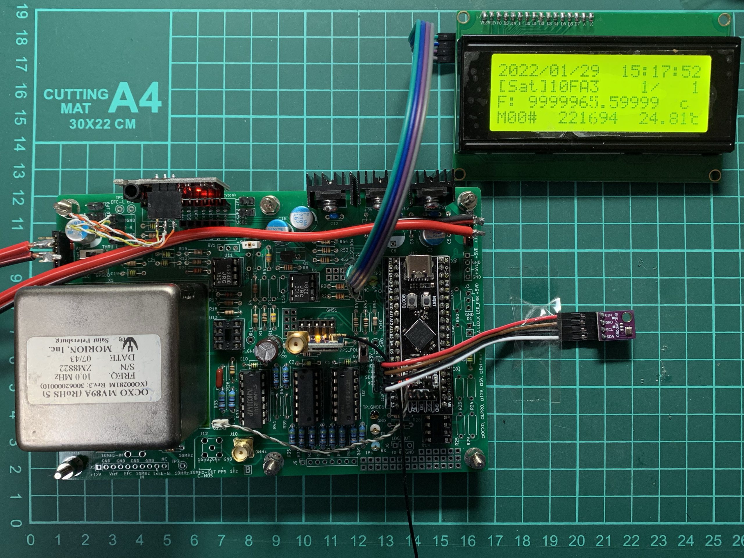
- Line #1: Date & time. A time zone is a compile option. (UTC and JST version are provided.)
- Line #2: Day of the week. GPS status, number of satellites in view, lock status fix, 2D or 3D.
Integration(Gate) time to measure frequency and phase drift. - Line #3: Estimated frequency in MHz which measured previous integration(gate) period.
- Line #4: EFC DAC value. Temperature, measured by BME280.
To get stability and precision, highly recommend to keep the power on. Frequent power on and off may cause damage OCXO.
Copyright and other Legal terms,
THE CONTENT IS PROVIDED ON AN “AS-IS” BASIS WITHOUT WARRANTY OF ANY KIND. YOU USE IT AT OWN YOUR RISK.
We are not liable for damages which you, or anyone else, directly or indirectly suffer because you use this web information.
We grant to you use the web information, ideas, designs and documentations for non-commercial purposes. We keep Copyright.
HI,
please.
decode protocol NMEA or TSIP?
Tnx
Thank you for visiting my blog.
It decodes NMEA.
Any possiblity to get gerber file ?
Thank You
Thank you for visiting my blog and the comments.
I will send you the gerber by email.